Semiconductors at scale
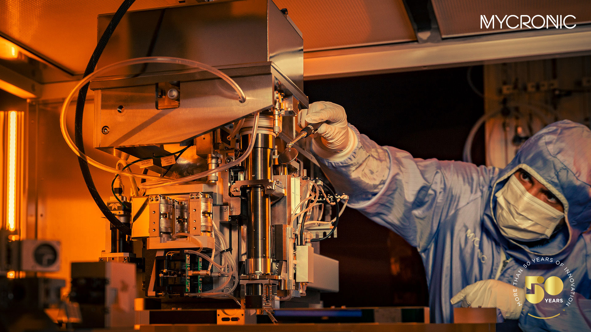
50 years of innovation - How an early innovation laid the template for today’s semiconductor photomask industry.In 1971, a group of Swedish engineers from the Royal Institute of Technology (KTH) began work on developing the first commercial laser mask writer. By the late 80s, Gerhard Westerberg and his team had sold their first system for the production of 6-inch photomasks for semiconductor applications. At the time few would have predicted that, a half-century later, it would be the foundation for a technology supporting the production of trillions of semiconductors worldwide.
The rise of semiconductors
Smart devices. Connected vehicles. Automated manufacturing. In a world where virtually every industry relies on computing power, semiconductor components are among the most critical building blocks in the modern economy.
Until recently, most of us took the production of Integrated Circuits (ICs), or “chips”, for granted. Our smartphones kept us connected.

Smart speaker.
Our car sensors kept us safe. And little thought was given to the extremely advanced manufacturing systems and capital-intensive investments that make all these devices possible. Then, in a matter of just a few years, supply chains were severely disrupted.
Tiny chips, big demands
For the major chip foundries, the global pandemic, trade disputes and rising demand for computing power all coincided in a perfect storm. Suddenly, new cars couldn’t be manufactured. Common household appliances were in short supply. And countless emerging technologies saw development slow down, and costs rise.

“Here I was in Japan, which for so long has been a leader in semiconductor technologies, and I was stuck waiting nine months for a new boiler for my home – all because a manufacturer couldn’t get their hands on enough chips. This goes to show you how deeply we all rely on the continued production of semiconductors.”
Keeping up the volume
Without photomasks, none of these critical components could be produced. Photomasks, which contain a master image of the chip design, are produced by either electron-beam or laser mask writers, depending on the geometry of the features on the chip. Some 500 systems produce photomasks for all the world’s ICs today. And more than 50 of them are built and served by Mycronic.
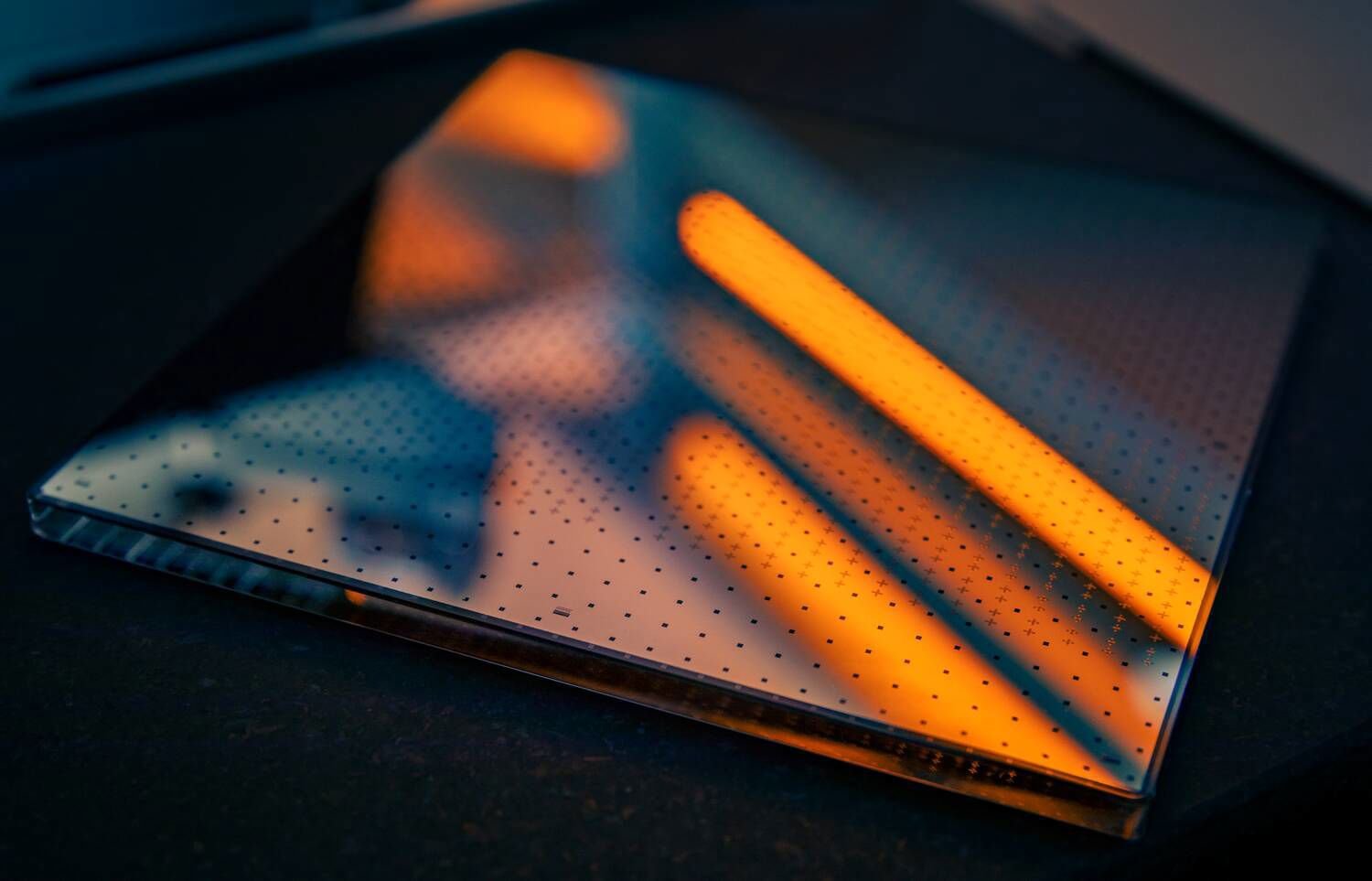
Photomask.
The majority of Mycronic mask writers for semiconductors are dedicated to the production of mature nodes, which are essential to industrial and automotive systems as well as for a wide range of sensors, memory chips, microprocessors and complex systems-on-a-chip (SoCs). Wherever possible, the mask writers are also used for advanced components, also known as “leading-edge” nodes, which are the most advanced ICs typically found in smartphones and consumer electronics.
“Today’s ‘leading-edge’ nodes are mostly done with electron-beam writers for critical layers,” explains Kenji. “They’re extremely precise and can produce nodes down to 15 nanometers in width, for 5-7 nanometer IC nodes. But they cost around 50 million euros and spend 6-10 hours to produce a photomask, compared to less than one hour with a laser writer. So the price-per-mask is many multiples higher. This simply won’t support the huge production volumes the world needs. That’s why around 70% of today’s photomasks are produced with the more cost-efficient and highly productive laser mask writers.”
Pushing the limits of laser technology
By the turn of the millennium, Mycronic had introduced a number of leading innovations through its Omega and Sigma series mask writers. One of these was a revolutionary deep-UV and spatial light modular (SLM) technology that enabled high-throughput pattern generation for, at the time, leading-edge nodes down to 65 nm.
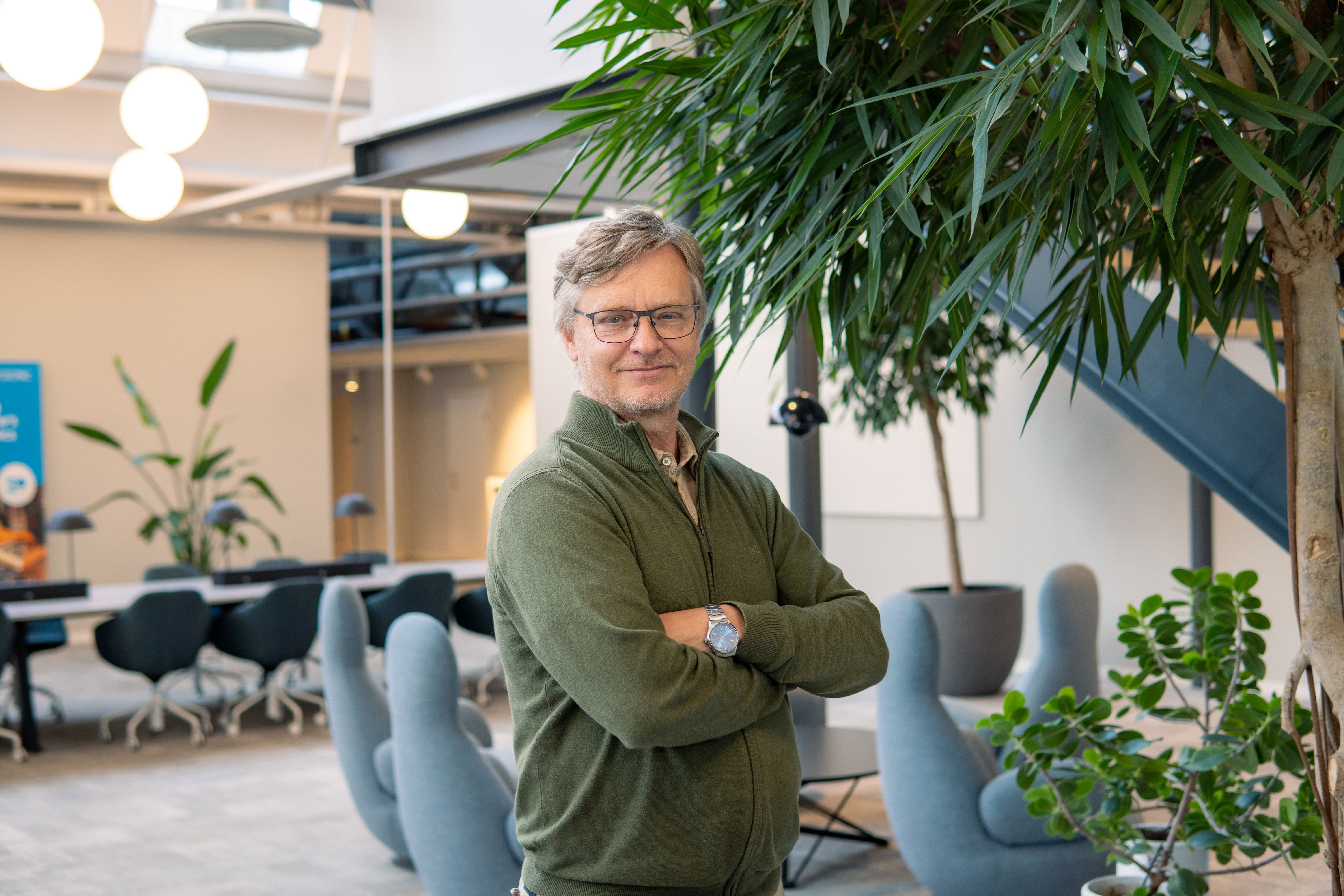
Mats Rosling, VP Tech Expert
"Sigma could write phase-shift masks, which was a major boost in resolution for the steppers using the photomasks,” says Mats Rosling, VP Tech Expert, Mycronic. “It was extremely innovative,” agrees Kenji, “and we sold systems to the major chipmakers. But it was expensive, and maybe even too innovative for its time.”
“By around 2010, the entire market had gone leading-edge – including us. This was the age of smartphones, laptops and mobile devices, which pushed much of the development and investments towards cutting-edge technologies for the production of advanced nodes. As a result, the mature node market became largely underserved.
Cutting-edge equipment for mature nodes
The SLX series mask writer emerged out of the demand for more advanced technologies in the mature node segment. Introduced in 2019, it applied up to two-digit laser beams to boost throughput speeds by three to four times, compared to many of the legacy systems currently in use today. “Most of the industry was reluctant to invest in this type of development,” explains Kenji. “But, thanks to our display mask writers, we could build on a state-of-the-art display technology that was quite suitable for certain mature nodes, so we didn’t need to start from scratch.”
The result was a more accurate and cost-efficient system than anything else available on the market. “It’s a perfect example of how we listen to customer demands and continue to introduce new products – and the industry gives us a lot of respect for this,” says Kenji. “Just couple of months ago at an industry event, one American customer stood up to tell everyone: ‘Mycronic is a very brave company. Nobody tried to develop a mature node machine. They were all afraid of price pressures. But someone had to do it, and Mycronic showed it was possible.’”
Supporting global production
The SLX series is now fundamental to the continued build-out of global chip production, as well as for the replacement of soon-obsolete mask writers worldwide. “The global landscape is changing,” says Kenji. “Twenty years ago it was all led by Japan and the US. Then there was outsourcing to Taiwan or Korea. Now Europe, Japan and the US are investing heavily, and China alone has close to twenty new photomask production sites.”
“Nowadays everyone recognizes that mature nodes are mandatory,” he continues. “It’s an inescapable fact. Without them you can’t produce ICs. So as chip production rises, the world will need more photomasks. And we will keep developing new machines and pushing the performance, which will continue to improve manufacturers’ capabilities as well as productivity.”
A world-class knowledge hub
From one machine in the late 80s to more than 50 systems in operation today, Mycronic has maintained its role as a global leader in laser mask writer expertise. “When I started we were just a small company with thirty people,” says Mats. “I remember I had to take all my books with me from my physics classes because then, as now, it really takes at least a year on the job just to understand the technology.”
As an example of the precision involved in developing these systems, Mats mentions a critical stage and mirror material which can only expand or shrink some 6 to 10 parts per billion for each degree Kelvin, according to SEMI standards. “This is an extreme level of thermal stability,” he says. “Otherwise, you’ll get print errors. So just to get materials like this, we’re competing for resources with some of the most advanced space mirror telescopes in the world.”
“It was also a major breakthrough to introduce the first solid-state laser,” he adds, “but it required two years together with our development partners just for the testing alone.”
At the heart of a strategic industry
The fact that so much of this expertise is gathered in one place in Sweden remains a source of pride for many at Mycronic. “It’s remarkable that everything is still built in Täby,” says Mats. “You have all the theory and practice in one place. We’ve collected a huge wealth of experience, which makes it fun to work here. Semiconductors have become a strategic business, so a big academic community has grown up around it. In my daily work, virtually everyone has a technical or commercial background. So if you’re interested in semiconductors, if you’re interested in everything from mechatronics and mechanical engineering to optics, software and system design, then there’s hardly a better place to be.”
Standing on the shoulders of giants
Despite Moore’s law, and despite the complexities of navigating a global semiconductor market now worth more than a half-trillion dollars, Mats Rosling is confident that Mycronic remains well positioned for the future. At the same time, he remains genuinely grateful for the foundations upon which the company’s technologies were built.
“The industry may have changed exponentially,” he reflects, “but the basic technology is still here. The patents for our original acoustic-optic deflector and modulator are still alive and well some 40 years later. So we’re really standing on the shoulders of the giants who invented these technologies decades ago at KTH. It’s not easy to be the first in something like this: a fundamental technology that has become the backbone of a whole new industry.”
Text: Grant Baldrige
FACTS
Each year Mycronic mask writers produce photomasks which support an industry that:
-
Produces around 330 billion semiconductor devices annually
-
Represents a market value of around 530 BUSD
Mycronic semiconductor mask writer history in brief
-
Early 1970s – A research team from KTH begins development of first commercial laser mask writer for semiconductor production
-
Late 1980s – Micronic Laser Systems installs the first LRS-18, the first commercial system at Align Rite, United Kingdom
-
Late 1990s – Omega series is released, selling more than a dozen systems for leading-edge node production
-
Early 2000s – Sigma series is launched, introducing breakthrough deep-UV and SLM technologies
-
2019 – SLX series is launched, selling more than 50 systems for high-volume mature node production