Design freedom at jet speed
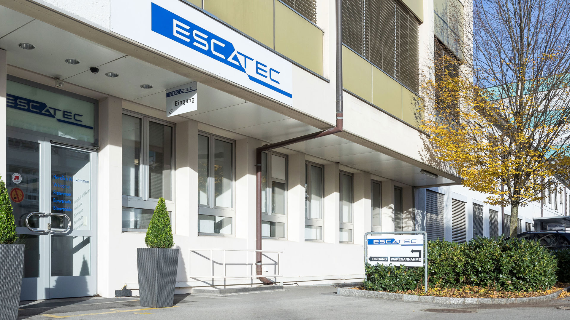
How ESCATEC accelerates new product cycles and boosts yields with the MY700At the ESCATEC facility in Switzerland, new products are being designed, prototyped and ramped up for full-scale manufacturing. Every day, two production lines churn out advanced electronics for high-power LED modules, LiDAR products, Time-of-Flight (TOF) modules and specialized camera systems. Once optimized for large-scale production, many are destined for commercial production at one of ESCATEC’s high-volume production sites in Bulgaria or Malaysia.
The springboard to full-scale manufacturing
ESCATEC’s production requires many highly technical iterations to develop processes for advanced solutions like chip-on-board technology, encapsulation and active alignment, demanding extreme levels of flexibility and process control. “We do a lot of design engineering and Design for Manufacturing (DFM) analysis here,” says Martin Mündlein, Production and Engineering Manager at ESCATEC Switzerland. “About 20% of our capacity is for NPIs, which aren’t just first runs but also products that need a few rounds to stabilize. They typically consist of 50 to 500 boards. The rest of our capacity is for series production of, say, 1,000 to 100,000 boards per year.”
To facilitate these rapid production ramp-ups, the Swiss facility has long relied on stencil printing of solder paste — the industry standard for high-volume production. But when it comes to fast-paced design changes and more complex assemblies, stencils alone can have their drawbacks.
A step too far for stencils
“For industrial electronics,” he explains, “you might have a lot of 0201 components and metal shielding (a stamped or embossed piece of metal). And then you need to add more solder paste to bridge the gaps, or add small dots of paste. We also do quite a few IoT and wearable devices, which have very small components placed with very high density on a combined flex/rigid board. Sometimes the chips are as small as 01005! And even with stepped stencils, all of these are incredibly tricky to produce.”
The nightmare board arrives
As an example, Martin mentions a particularly difficult PCBA for one of the company’s biggest customers. “It was an important, high-pressure project. There were 2,000 pieces in the first order, and we needed to use all the parts.”
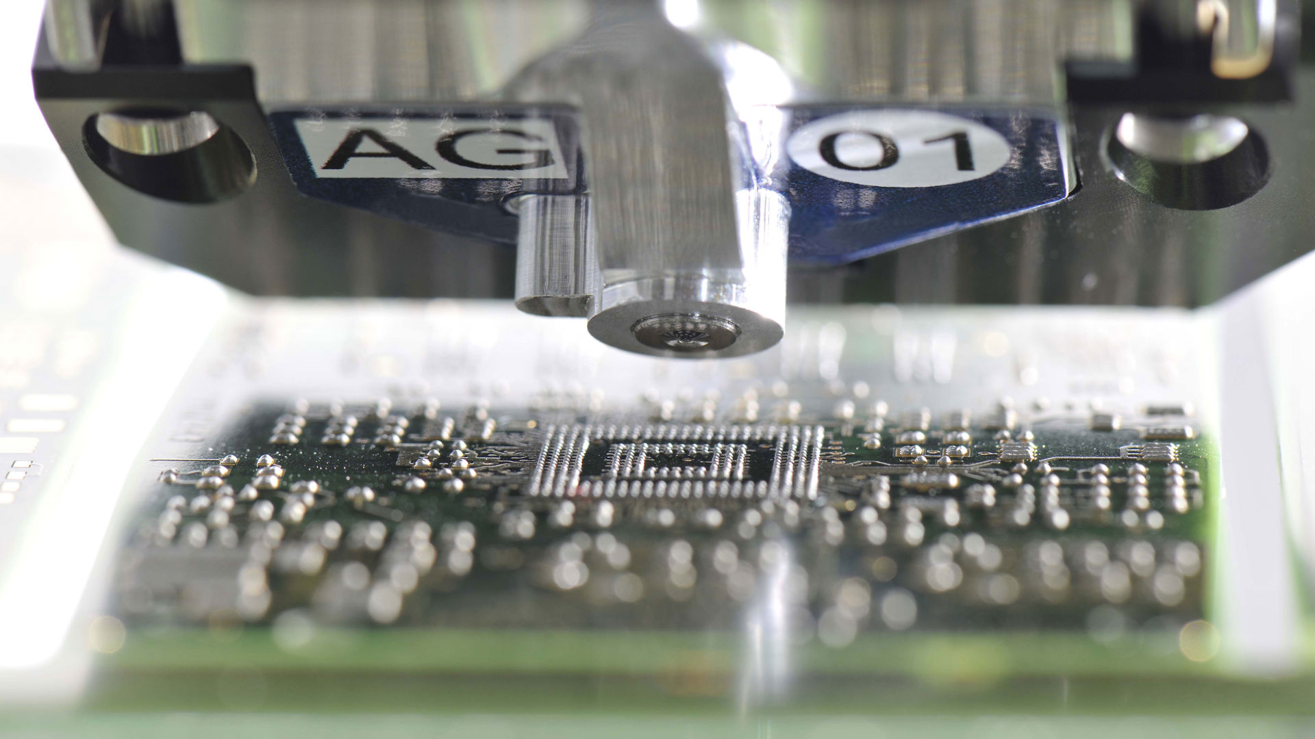
The problem was not just that the PCBA had an especially complex design, but that paste needed to be applied both in a top layer and a cavity. “It was a very fine-pitch board with fine-pitch connectors. This meant that some solder deposits needed to be less than 200 microns in size. In theory, you could step down to a few hundred microns on a stepped stencil, but it was a nightmare with the layout and format of this board.”
Nearly one year later, after several iterations, more than three stepped stencil designs, poor solder joint yield and a high scrap rate, Martin and his team realized there had to be a better way. In 2023, they decided to install a MY700 Jet printer as an add-on process step, following the screen printer, for some of the most difficult applications.

Weeks of time savings
This problematic board was one of the first tests to be run through the line. “We tested it on the Jet printer and immediately saw the advantages of being able to print on two layers and quickly adapt the designs,” says Martin. “It’s opened up a lot of design freedom that we didn’t have before. So now, if a stepped stencil is involved in a new product, it’s much easier to go straight to the Jet printer. Then, if it makes sense from a maturity or cost perspective, we’ll switch it over to the stepped stencil.”
“Best of all,” he adds, “the iterations are all on-line, so in just this one case it could have saved us weeks, or even months!”
These time savings, says Martin, might just be the biggest advantage of jet printing in general. “Lead times can really benefit a lot,” he says. “Because a new stencil takes two or three days to arrive, and then another couple of weeks to adjust the process and get it running in the line. This can have major cost implications as well. Sure, the stencil maybe costs 200 Euros, but then you have to wait a few days for the line to become available between batches, adjust, experiment and wait again. And that can add up to a lot of lost productivity.”
In just this one case, it (Jet Printing) could have saved us weeks, or even months.
Reducing waste
In the early phases of prototyping, every iteration also contributes to significant material waste. “We have a huge scrap metal bin,” says Martin. “We’re talking about hundreds of single-use stencils from the prototypes. And now, with the Jet printer, I can definitely say that this pile is much smaller.”
Even more valuable, of course, are the boards and components themselves. Asked whether the Jet printer has influenced these scrap rates, Martin responds: “In the case of that cavity board I mentioned earlier? For sure. With the stepped stencils we had to scrap around 10% of boards. Now our scrap rate is close to 0%.”
Martin is careful to mention that this is far from a general rule, however. “Keep in mind that this was a really tricky board,” he explains. “In most cases, about 80-90% of the time, we hit the mark with a stencil the first time.”
Turning up the dial
Naturally, for ESCATEC, jet printing will never fully replace stencil printing. In a company where ultimate flexibility is required by customers to support prototype builds through to mass production, with potential volumes reaching millions of boards per year in multiple locations, the speed of screen printing is still essential.
But from where Martin stands, overseeing a highly design-driven R&D and manufacturing environment, the MY700 represents a versatile new tool in his SMT toolkit. “Our manufacturing team loves the machine,” he says. “They’re constantly faced with customers who have a functional principle and say: ‘Can you make a product out of this and manufacture it?’ Or they have to optimize a semi-finished product from functional samples. In both cases, they need to quickly adapt and optimize a product, and the MY700 is perfect for this.”
“At the end of the day,” he continues, “the more screws we can turn to fine-tune the process, the faster we can respond with better yield, consistency and quality. And jet printing really helps us turn it up a notch.”
ESCATEC in brief
Locations: Malaysia (Group HQ), Switzerland, United Kingdom, Czech Republic, Bulgaria
Group employees: 2,000+
Core markets: Transportation, industrial and medical electronics
Services: EMS Design & manufacturing including embedded software, hardware design, DfX, microelectronics, PCBA, box build, mechatronics and more
Total SMT lines: 15