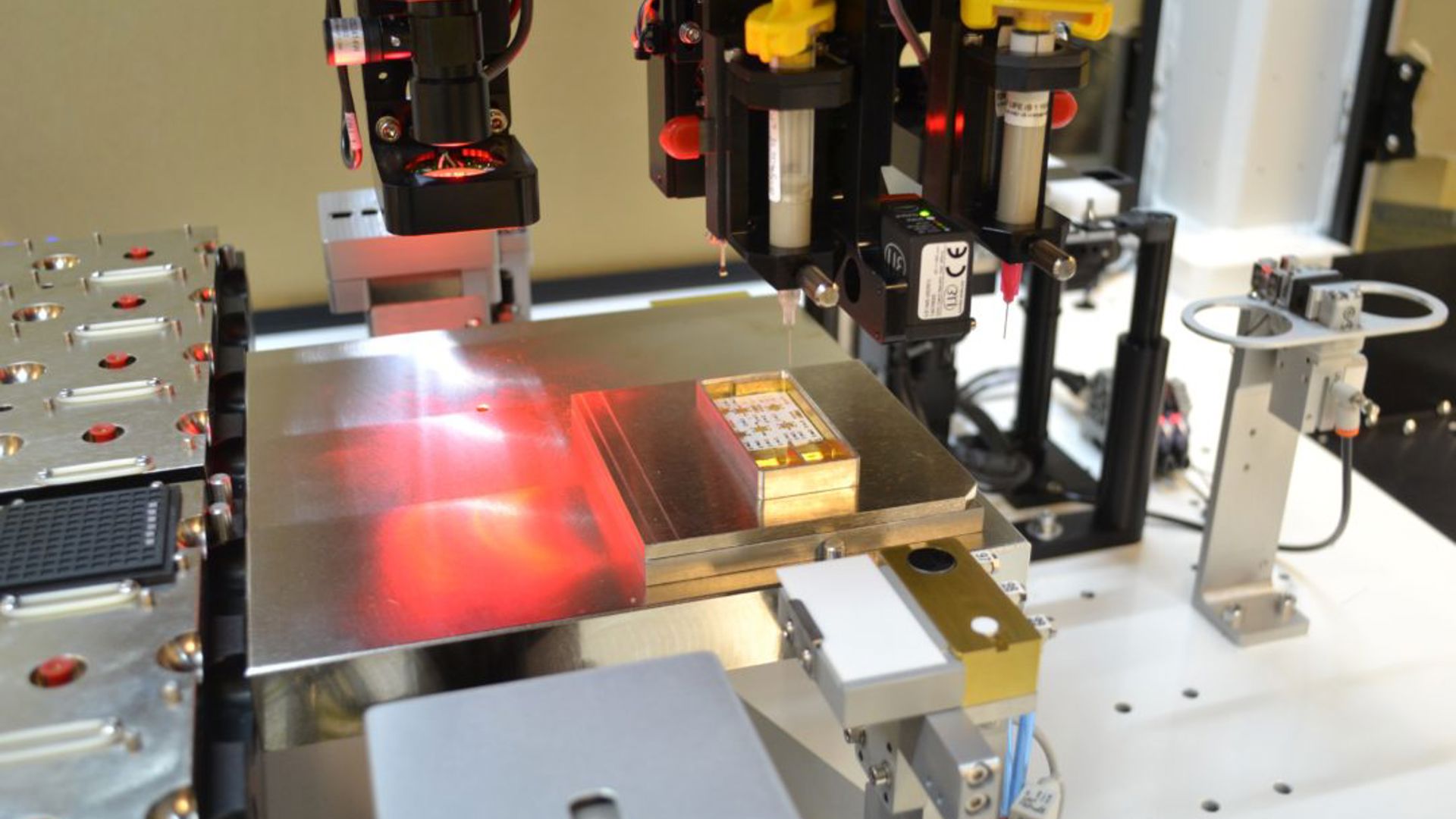
Die Bonding Process Pages – Highlights
Last quarter, we published some of the key processes that our fully automated die bonding systems are able to perform. Below we share some extracts from the three key sections:

Die Bonding can thereby be succinctly described as the placement of a semiconductor device onto the next level of interconnection, whether it be a substrate or a board. It is referred to in the industry as die placement, die attach, or die bonding. Although the objective is the same, die bonding processes and die bonding equipment vary greatly, depending on functionality, cost, performance, size, hermeticity, product life expectancy, and required reliability.
Various die bonding approaches have been, and still are, developed to meet the ever-evolving product requirements. Such approaches include:
- Epoxy Die Bonding combined with either batch, continuous or in-situ curing
- Eutectic Die Bonding and in-situ reflow
- Flip Chip Attachment combined with either standalone or in-situ curing
Eutectic die bonding sometimes referred to as eutectic die attach, is a die bonding technique used for devices that require enhanced heat dissipation, such as high-power amplifiers. The technique is also used when the outgassing of traditional die bonding epoxies is of concern. Gold-tin, gold-germanium, and gold-silicon are three common eutectic alloys. In simple terms, the eutectic die bonding process is automated by placing the package or substrate on, or moving it to, a surface that can be thermally controlled. The automated system then sequentially places the solder preform and a die onto the substrate. The temperature is then ramped up to achieve reflow. Ideally, temperature ramps are performed quickly for throughput and quality reasons. The process must occur in an inert environment to avoid oxidation. A void-free bond is obtained by using a technique called scrubbing. Below we outline the details of the eutectic die bonding process including an automated system using an in-line method of processing multiple parts simultaneously.
Epoxy die bonding sometimes referred to as epoxy die attach, is the most widely used die bonding technique in semiconductor assembly. Typical integrated circuits devices (ICs) have the circuitry layer built up on a base. Most of the devices interconnect to a module-level substrate by bonding a metal wire from the top surface of the IC (wire bond pad) to the surface of the substrate. Thus, the backside of the die can be used to attach the IC to the substrate using a bonding material. The most common die-bonding material is epoxy-based. Once the die is attached to the substrate in such a fashion, the assembly is usually cured, crosslinking based on a material-specific thermal profile.