High Volume Manufacturing of Photonic Devices: Assembly Starts with Design
The explosive growth of internet traffic demands higher bandwidth in data communications. High volume manufacturing of photonic devices is crucial to meet this demand, particularly fueled by hyperscale data centers. Further integration of photonics and electronics will pave the way for other emerging applications such as LiDAR, sensors for VR/AR, etc.

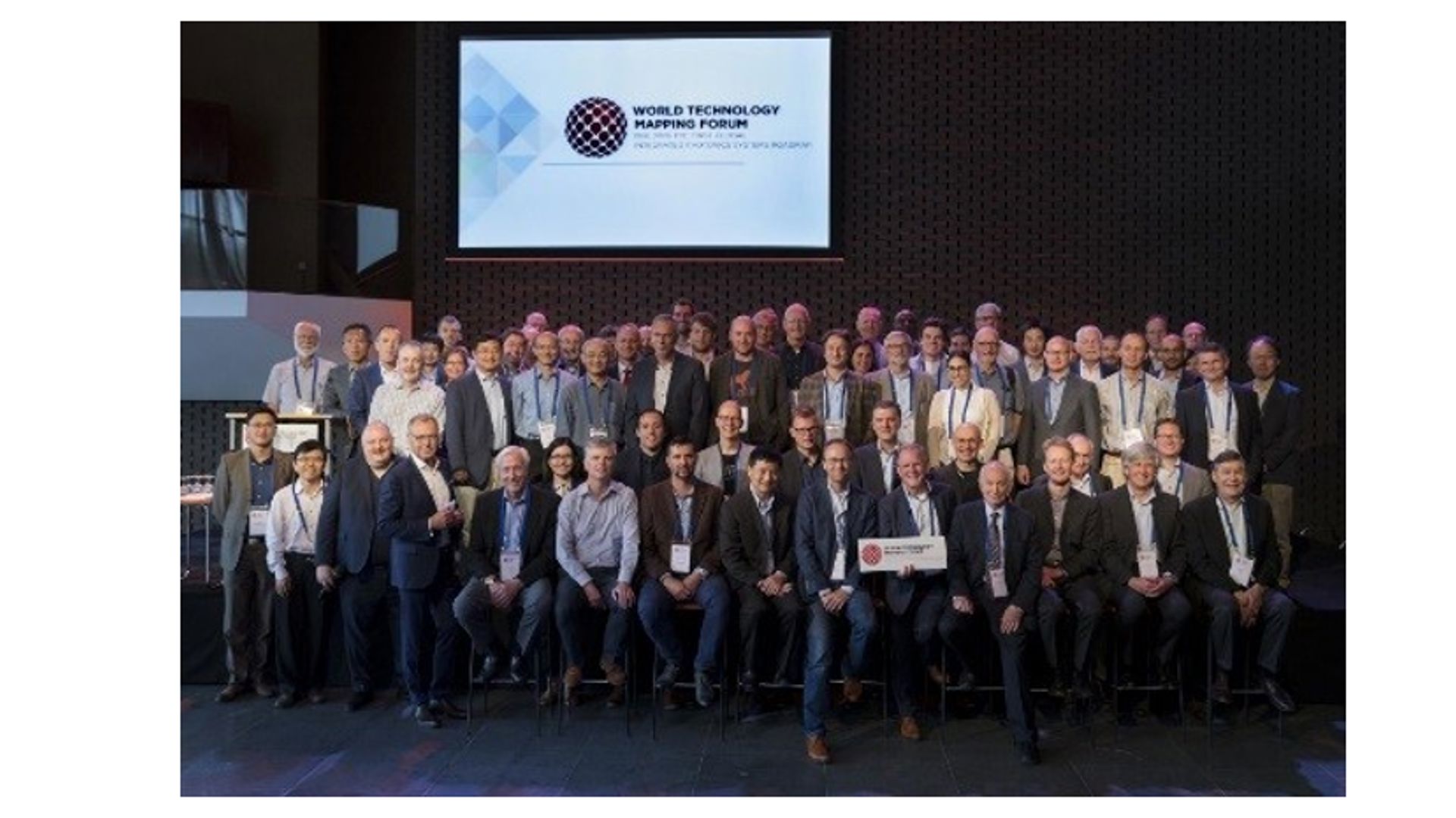
The unprecedented need for a high volume of photonic devices presents unique challenges in manufacturing. This was one of the key topics in the 1st World Technology Mapping Forum held in s’Hertogenbosch, The Netherlands, in June this year. Over 170 experts from 17 countries/regions attended the conference. MRSI Systems’ VP of Product Management, Dr. Yi Qian, co-chaired the Assembly Technical Working Group (TWG) Meeting and then presented the team’s findings and participated in the panel discussion. Dr. Qian also presented the earlier studies on behalf of the Assembly TWG of The Integrated Photonic System Roadmap (IPSR) initiative / AIM Photonics Academy, where he is also the TWG co-chair.
One of the key findings from the forum was that high volume manufacturing and assembly of integrated photonic device needs to start with design. Oftentimes, some might have thought that the assembly process is only for the manufacturing team. In turn, designers may not think of assembly in terms of yield and throughput. Now, with increasing volume and more automation, planning for assembly processes needs to start at design. For example, alignment marks defined by precision lithography on a laser chip and on a heat sink submount can help an automatic die bonder vision more readily vision align and thus more accurately position the two parts. The results are improved reliability (accuracy) and higher throughput. Assembly throughput increases significantly because the vision system is able to more successfully capture alignment marks made by precision lithography than those images based on die edges and overall shapes. Those edges could be pretty rough and the shapes can be hard to recognize by the vision system.

Another point of the key findings was that photonics high volume manufacturing systems must be fast, accurate, and flexible. Why? Those attributes are needed to satisfy the unique requirements of photonic devices that have a more complex design, less standardization in packaging, and multiple parts with various sizes and geometries. For example, an electro-absorption modulated laser (EML) may need to have two to four capacitors, one thermistor, one back-fact power monitor, and one laser chip on the heat sink platform. To make things more complicated, some parts need to be bonded eutectically, but other parts need to be epoxy-bonded. One die bonding machine needs to handle both die bonding processes within its picking and placing steps. In simple terms, this die bonder must not only be high speed but be capable of multi-chip, multi-process production.
Stay tuned with more discussions from MRSI on these trends, challenges and opportunities for high volume photonic manufacturing.
Learn more about AIM Photonics Academy.
Learn more about The Integrated Photonic Systems Roadmap.
Learn more about World Technology Mapping Forum.
Learn more about new product MRSI-HVM3 at MRSI Systems.
About MRSI Systems
MRSI Systems is a leading manufacturer of fully automated, high-precision, high-speed die bonding and epoxy dispensing systems. We enable customers to optimize the performance of their process including yield, throughput, and uptime by building systems that use our unique expertise. In summary, this includes our proprietary software, proven hardware, deep process knowledge, state-of-the-art manufacturing, and a world-class customer service team. MRSI’s systems are built on common platforms that can be configured to meet specific customer requirements. These platforms are designed to be scalable for R&D prototyping, pilot production and high volume manufacturing. Our solutions deliver the best financial returns in the industry while integrating seamlessly into our customer’s production. Markets include Telecom/Datacom (Data Center), Aerospace & Defense, Medical Devices, Computers and Peripherals, and Industrial. Since 1984, we have been recognized as the standard of the industry, delivering our solutions to leading optoelectronic and microelectronic customers worldwide. We are headquartered in Billerica, MA in the greater Boston area. Our sales are supported by a global network of direct service and support professionals, located in China, Taiwan, Singapore, Korea, Thailand, Malaysia, the Philippines, Israel, Europe, United Kingdom, and the United States.
