LIDAR & AR/VR/MR
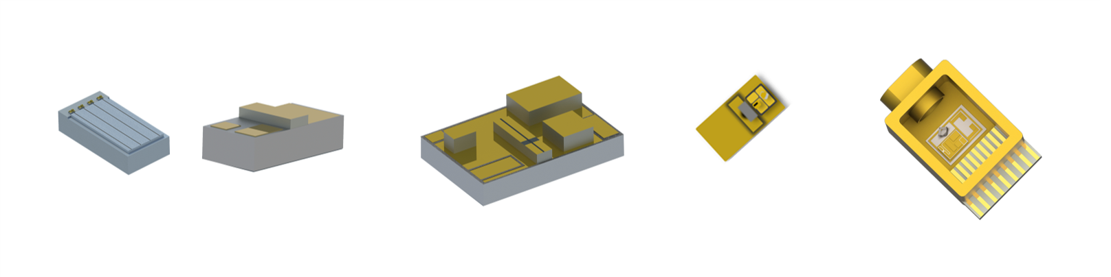
LiDAR devices do not use standard packaging because different customers have different packaging designs. Similar to an Optical Communication device, a LiDAR package also includes a laser light source, photodetector, optical elements, and IC chips. However, current LiDAR devices have more chips and components than the optical communication devices. The package consists of many different kinds of CoBs. The manufacturing process uses more high precision dispensing and stamping of epoxy. Some use eutectic and UV process. Flexible multi-die and multi-process die bonding machines with high speed and high accuracy are the best sol
For AR/VR/MR hardware, the die attach process uses epoxy or stamping processes with high accuracy. AR/VR/MR also demands the ability to handle both big and small die to build the device. Currently, most AR/VR/MR products are still in prototype or small volume manufacturing and the process is changing frequently. Flexible assembly equipment is the best fit for these applications.
Die Attach
- Eutectic
- Epoxy stamping
- 0.5μm, 1.5μm, 3μm, 5μm
- Chip-on-Carrier (CoC), Chip-on-Submount (CoS)
Lens Attach
- UV epoxy dispensing
- In-situ UV curing
- Placement accuracy options: 1.5μm, 3μm, 5μm
- Passive Optical Alignment
Gold-box Packaging
- Thermal and UV Epoxy
- Eutectic
- Placement accuracy options: 1.5μm, 3μm, 5μm